语言选择:


FSTN LCD screen, liquid crystal display module
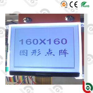
General Specification:FSTN (Film+STN), in order to improve the background color of the ordinary STN, a compensation film is added on the polarizer to eliminate the dispersion and realize black and white display.Can be made into blue, green, orange, yellow, and other colors of the screen background.The following are 160*160 parameters for reference:
|
Item |
Description |
Unit |
|
Outline Size(mm) |
80.0(L)×72.5(W)×5.0(T) (Not Include Connector) |
mm |
|
LCD Type |
FSTN, Transflecitve/Positive, 1/160Duty, 1/10Bias |
--- |
|
Display Type |
160×160 dots |
--- |
|
View Area |
60.00×60.00 |
mm |
|
Display Area |
54.38×54.38 |
mm |
|
Dots Size |
0.32×0.32 |
mm |
|
Dots Pitch |
0.34×0.34 |
mm |
|
Controller & Driver |
UC1698U (COG) |
--- |
|
View Direction |
6 O’Clock |
--- |
|
Interface Mode |
8 bit 6800,8 bit 8080 |
--- |
|
VDD&VOP(Type) |
3.3 V & 16.3 V |
V |
|
Backlight Color |
White, 3.0V, 90mA |
--- |
|
Operation Temp. |
-20~+70 |
℃ |
|
Storage Temp. |
-30~+80 |
℃ |
Pin Connections
|
Pin No. |
Pin Out |
Description |
|
1-2 |
NC |
No connection. |
|
3-4 |
VLCD |
High voltage LCD Power Supply. When internal VLCD is used, connect these pins together. When external VLCD source is used, connect external VLCD source to VLCDIN, pins and leave VLCDOUT open. |
|
5 |
VS+ |
LCD Bias Voltages. These are the voltage sources to provide SEG driving currents. These voltages are generated internally. Connect capacitors of CAX / CBX value between VAX+ / VBX+ and VAX– / VBX–, respectively. |
|
6 |
VS- |
|
|
7 |
VB0- |
|
|
8 |
VB1- |
|
|
9 |
VB1+ |
|
|
10 |
VB0+ |
|
|
11-12 |
VDD |
Power supply for LCD circuit. |
|
13-14 |
VSS |
Ground. |
|
15 |
BM0 |
Bus Mode: The interface bus mode is determined by BM0 with the following relationship: BM 0:Mode 1:6800/8-bit 0:8080/8-bit |
|
16 |
CS0 |
Chip Selection. Chip is selected when CS0 = “L”. When the chip is not selected, DB [7:0] will be high impedance. |
|
17 |
A0(CD) |
Selects Control data or Display data for read/write operation. In S9 mode, CD pin is not used. Connect to VSS when not used. |
|
18 |
WR1(RD) |
WR[1:0] control the read/write operation of the host interface. See section Host Interface for more detail. |
|
19 |
WR0(WR) |
|
|
20 |
RST |
When RST=”L”, all control registers are re-initialized by their default states. Since UC1698u has built-in Power-ON reset and software reset commands, RST pin is not required for proper chip operation. |
|
21 |
DB0 |
Bi-directional bus for parallel host interface. |
|
22 |
DB1 |
|
|
23 |
DB2 |
|
|
24 |
DB3 |
|
|
25 |
DB4 |
|
|
26 |
DB5 |
|
|
27 |
DB6 |
|
|
28 |
DB7 |
 东莞必步克
东莞必步克 东莞必步克
东莞必步克
 东莞必步克
东莞必步克